No single invention changes the world by itself. It must be made reliable, manufactured at scale, paid for, and woven into human life.
Historical narrative adapted from Chris Miller, Chip War (2022).
World War II
Industrial power meets information
Factories still decided how many aircraft, ships, and tanks a nation could deploy. But radar, rockets, cryptanalysis, and precision instruments showed that calculation was becoming military power too.
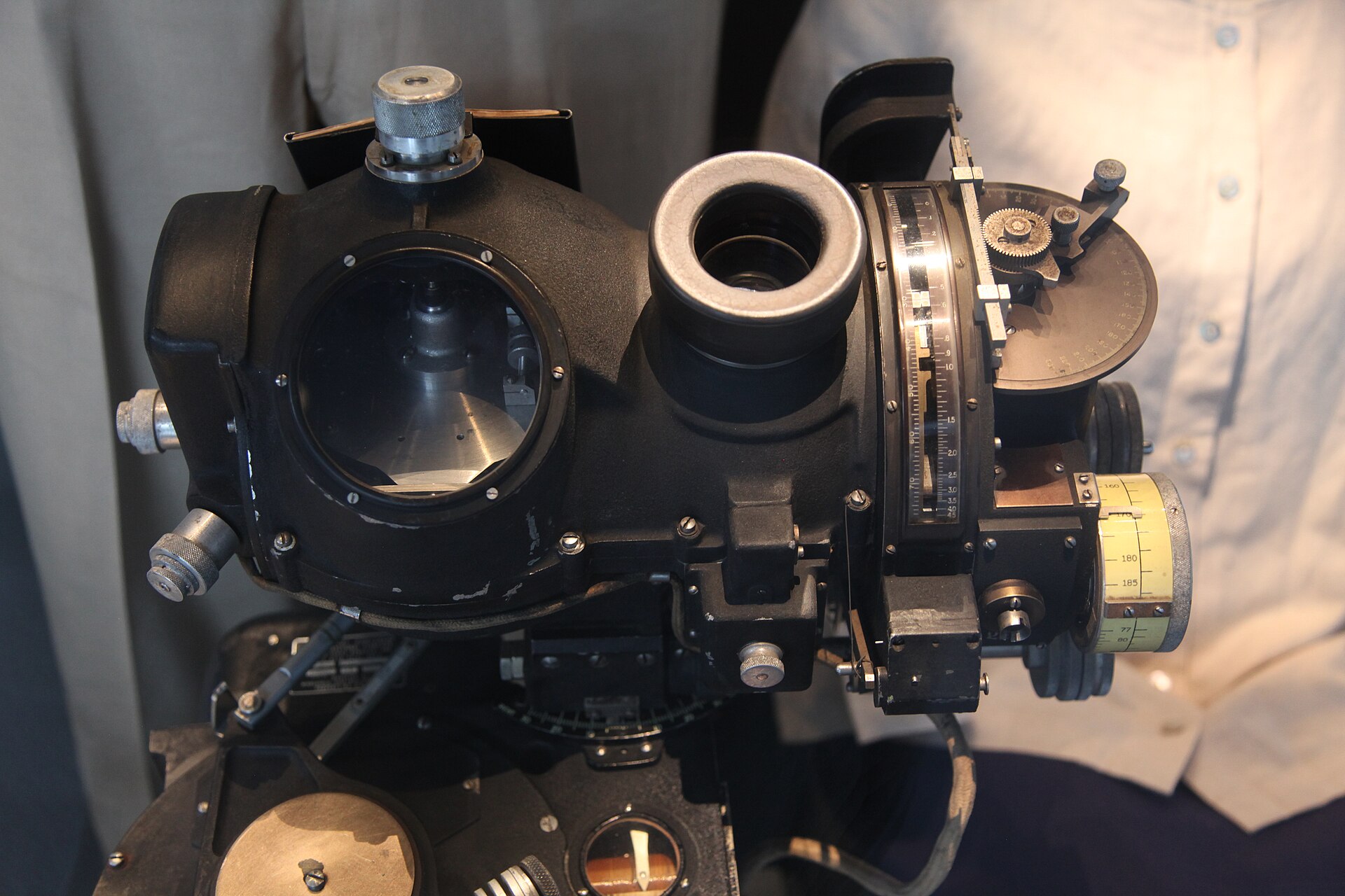
A mechanical bombsight combined altitude, airspeed, wind, and geometry to estimate when a bomb should be released.
A wire carries current and a resistor limits it, but neither lets one small signal control another, larger signal.
A triode vacuum tube introduced the crucial new ability: a small voltage at its control grid could regulate a much larger current, with no moving contact. It could therefore amplify a weak signal or act as a fast electronic switch.
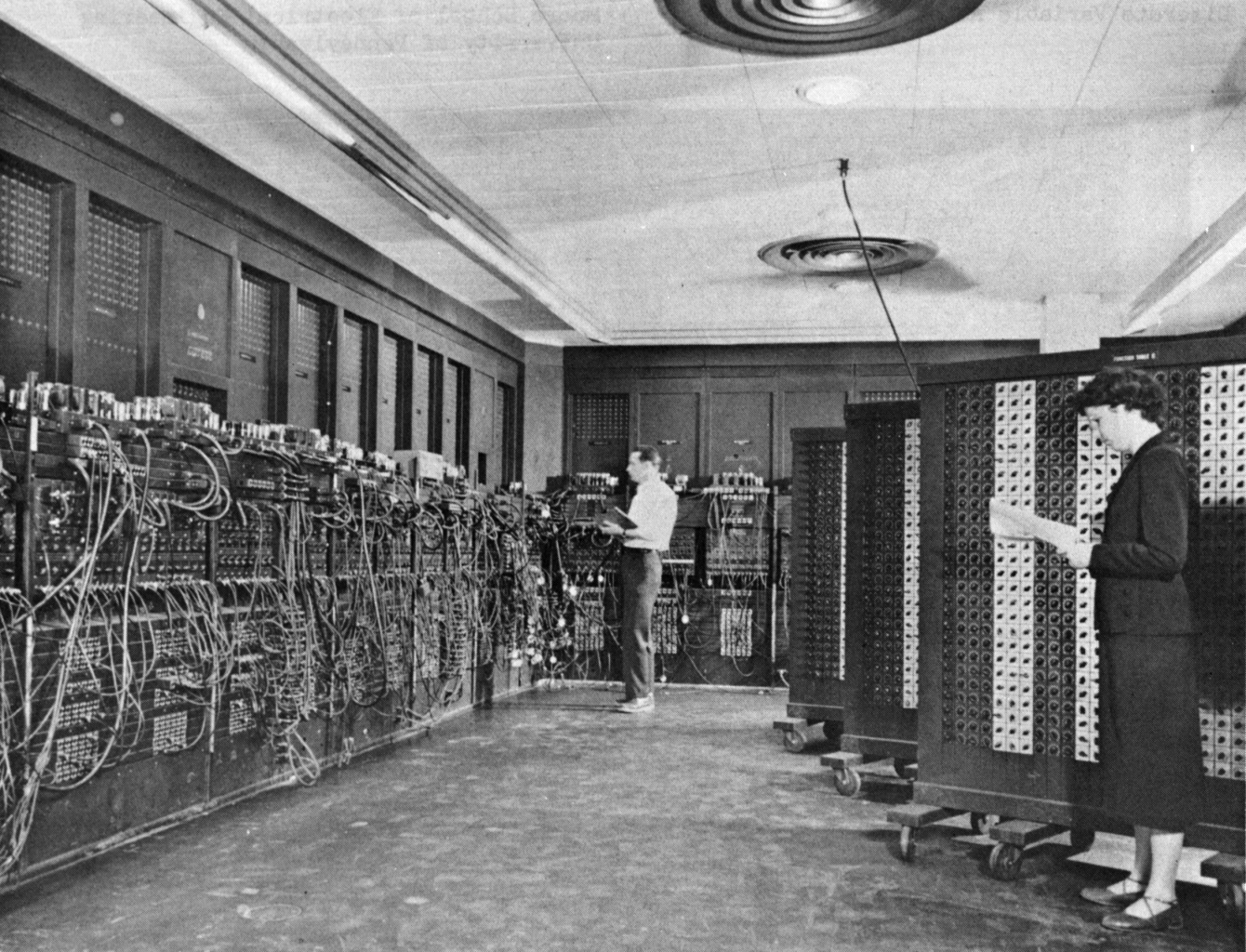
ENIAC used roughly 18,000 such switches, gaining electronic speed at the cost of heat, power, size, and reliability.
Betty Snyder and Glen Beck program ENIAC, circa 1947.
U.S. Army photograph, public domain.
The engineering question
Could a solid replace a vacuum tube?
Vacuum tube
Glass enclosure and heated filament
Bulky and power hungry
Difficult to pack densely
Semiconductor device
No heated filament
Electrical behavior can be controlled
Can be made tiny at scale
William Shockley believed the next switch would be built from a semiconductor: a material whose conductivity can be deliberately changed.
Bell Labs
Brilliance, collaboration, and rivalry
Shockley was a gifted theorist and an abrasive colleague. In 1945 he proposed controlling current through silicon with an electric field, but his experimental device produced no useful measurable result.
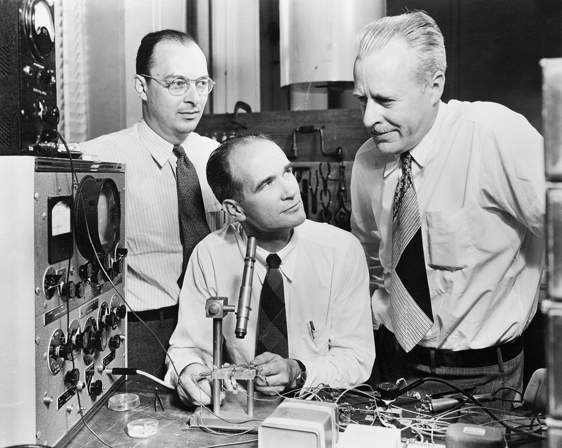
John Bardeen's theoretical insight and Walter Brattain's experimental skill found a different route through the problem.
Shockley's field-effect concept had failed experimentally.
→
Trigger
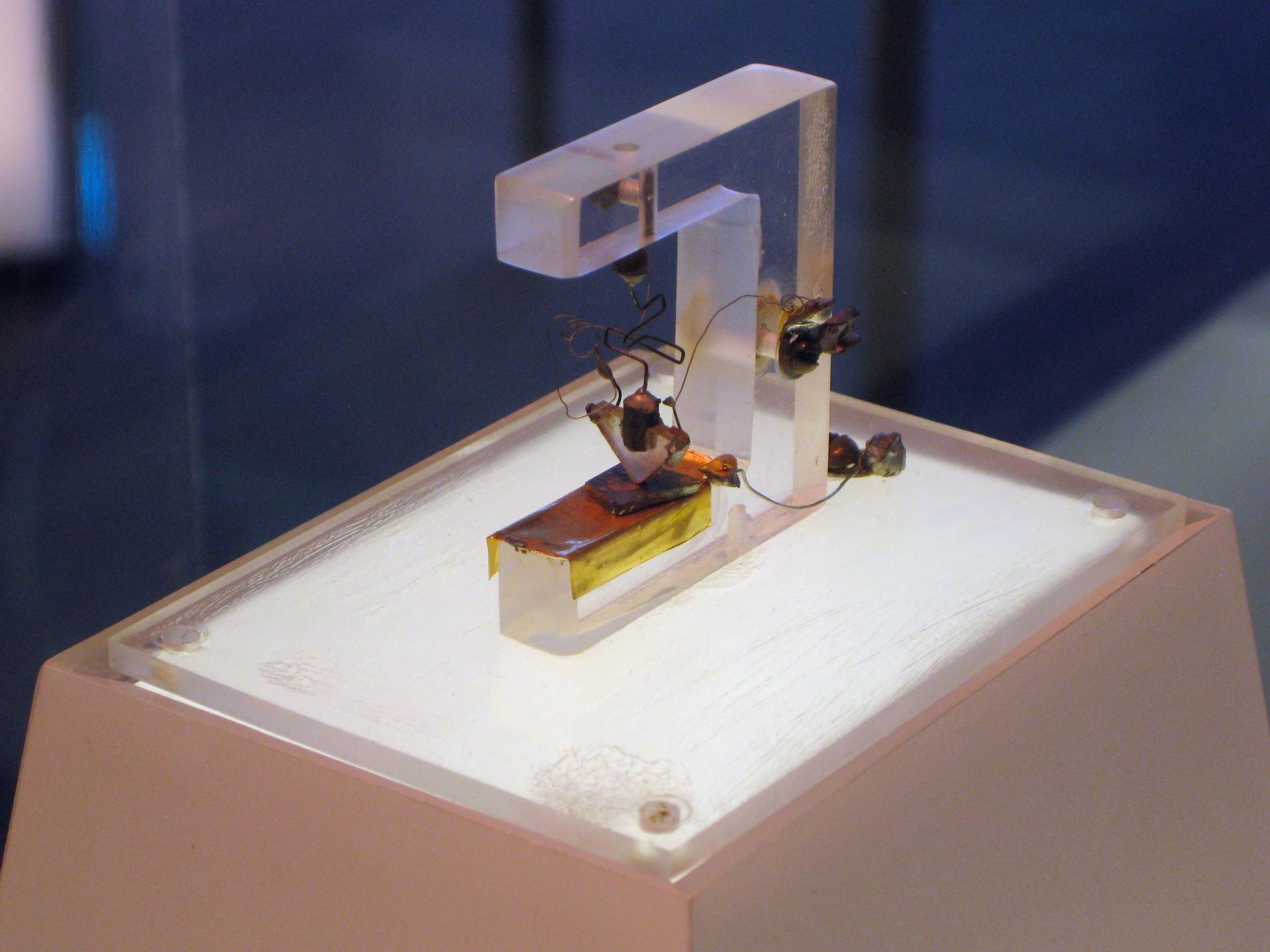
Bardeen and Brattain demonstrated transistor action first.
→
After
Working intensely and privately, Shockley conceived the junction transistor.
His three-layer semiconductor “sandwich” could use a small input to control a much larger current: amplification, and also switching - on, off, on, off.
A human invention
Who invented the transistor?
Research direction
Shockley
Led the Bell Labs group and pursued a solid-state amplifier; after the point-contact breakthrough, he conceived the junction transistor.
Physics and design
Bardeen
Explained the surface-state barrier that defeated the earlier field-effect idea and co-developed the point-contact transistor.
Experimental invention
Brattain
Designed and refined the experiments with Bardeen, creating the contacts that produced reliable amplification.
1956 Nobel Prize in Physics: Shockley, Bardeen, and Brattain shared the prize for semiconductor research and the discovery of the transistor effect. Nobel Prize record
Invention is only step one
A laboratory device is not yet an industry
1Works once
A researcher demonstrates the effect.
2Works reliably
Engineers control materials and processes.
3Can be repeated
Factories achieve acceptable yield.
4Becomes affordable
Volume lowers cost and creates markets.
The decisive contest moved from discovering transistors to manufacturing millions of nearly identical ones.
California, 1956-1968
Birth of Silicon Valley
Shockley left Bell Labs and founded Shockley Semiconductor Laboratory in California. He recruited exceptional young engineers, then drove eight of them away through suspicion and poor leadership.
The "traitorous eight" founded Fairchild Semiconductor and helped create Silicon Valley's startup culture.
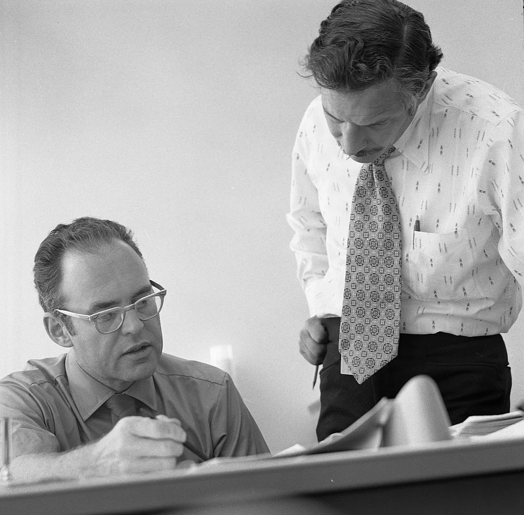
Robert Noyce and Gordon Moore later left Fairchild to found Intel: “integrated electronics.”
Further reading: Michael S. Malone, The Intel Trinity, on Robert Noyce, Gordon Moore, Andy Grove, and the making of Intel.
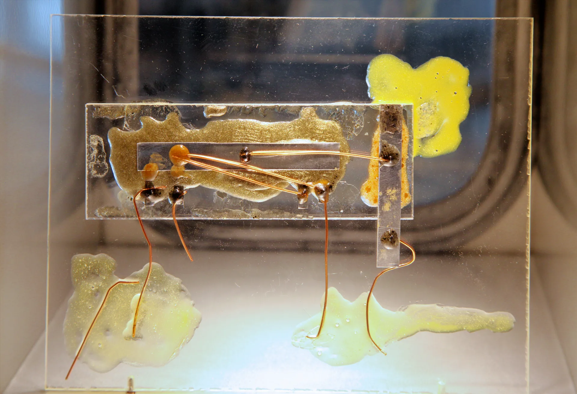
Working independently, Jack Kilby and Robert Noyce eliminated the need for wires to connect transistors.
This made the silicon integrated circuit practical to manufacture at scale.
Although Kilby and Noyce are recognized as co-inventors of the integrated circuit, Noyce did not receive the Nobel Prize because he died before the prize was awarded.
2000 Nobel Prize in Physics: Kilby received half of the prize for his part in inventing the integrated circuit. Nobel Prize record
Jay Lathrop and James Nall pioneered photolithographic techniques for semiconductor devices. Their work turned photographic patterning into a repeatable chipmaking method.
Coat: cover the wafer with light-sensitive photoresist.
Expose: project a circuit pattern through a photomask.
Develop: reveal selected regions of the pattern.
Process and repeat: etch or add material, one layer at a time.
Credit: Lathrop and Nall filed their semiconductor photolithography patent in 1957.
High value was placed on smaller size, lower weight, and guidance capability.
→
LearningFactories improve yield
Each production run teaches engineers how to reduce defects and cost.
→
Mass marketComputers and consumer devices
Falling prices create new uses, which drive still greater production.
A self-reinforcing cycle
Smaller, cheaper, more widely used
Better processes
→
More transistors per chip
→
Lower cost per function
→
New markets and volume
↺
Moore's Law described the industry's repeated increase in integrated-circuit complexity. It was not a law of nature; it became a shared target for an enormous industrial ecosystem.
The story becomes global
Hard problems were solved across the world
United Statestransistor, integrated circuit, chip design
Soviet Unionsemiconductor science and space electronics
Japanportable consumer electronics
South Koreamemory manufacturing at scale
Taiwanthe dedicated chip foundry
Netherlandsadvanced lithography machines
Chinatelecom systems and 5G equipment
No single country mastered every layer. Different communities solved different scientific, manufacturing, and systems-engineering challenges.
Soviet Union
The danger of a “copy first” strategy
The USSR had world-class physicists and made major achievements in space and semiconductor research. Its microelectronics system, however, was secretive, centrally directed, and heavily oriented toward copying foreign designs.
Replication can close yesterday's gap. It is much less effective when manufacturing knowledge and designs are changing continuously.
Manufacture for everyone, compete with no customer
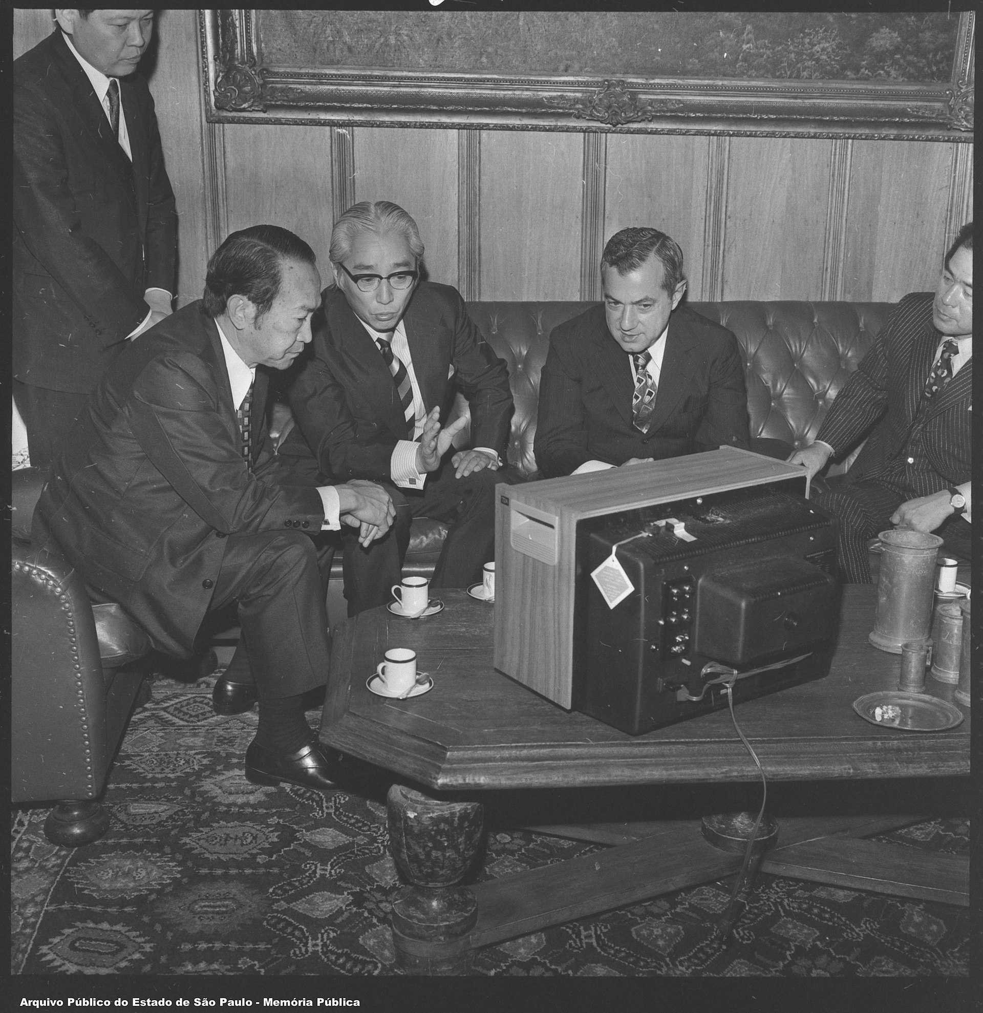
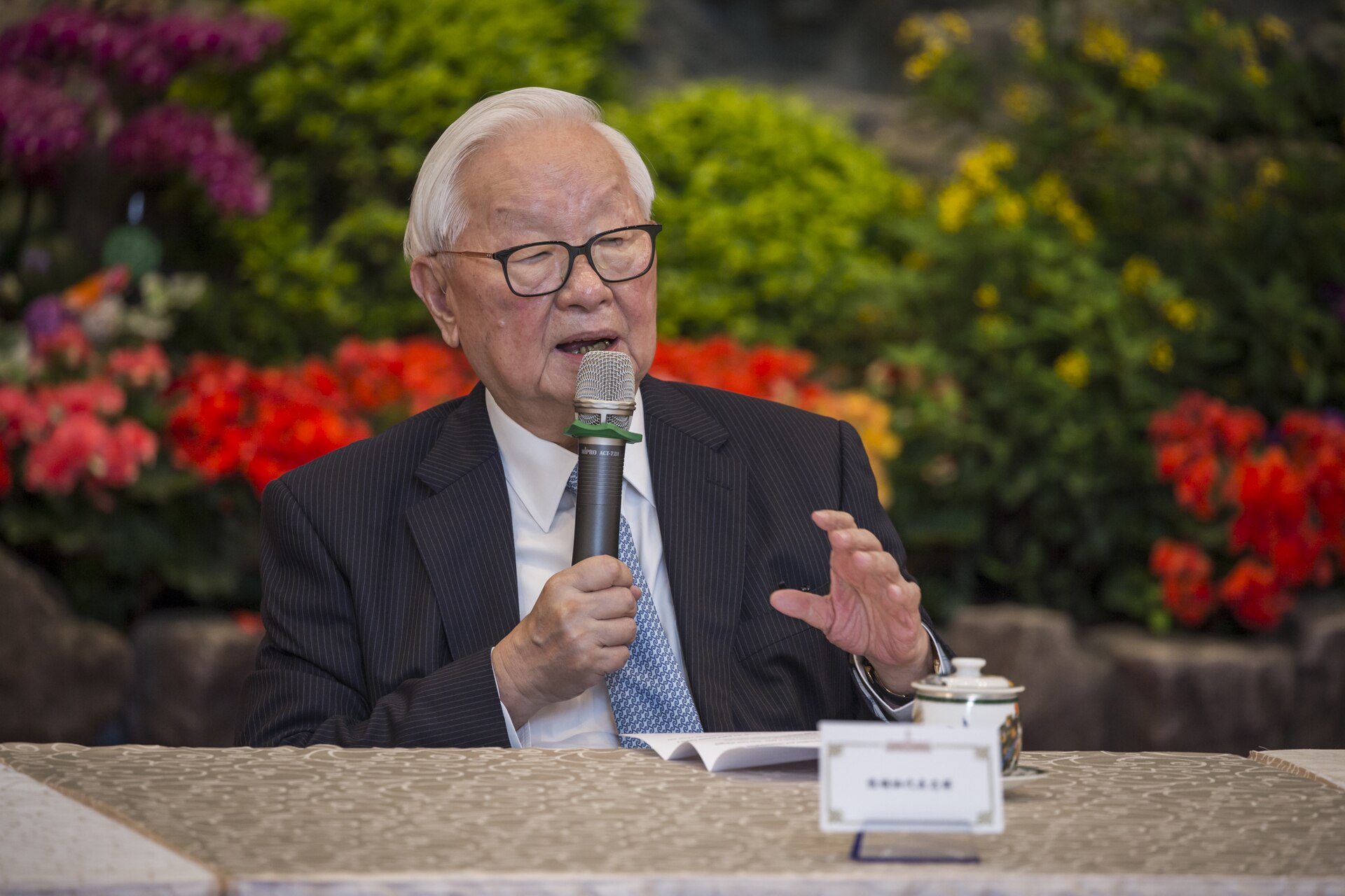
Morris Chang proposed a dedicated foundry: TSMC would manufacture chips designed by other companies instead of selling competing chip designs of its own.
The model lowered the cost of starting a chip-design firm. It also concentrated advanced manufacturing expertise in one extraordinary company and island.
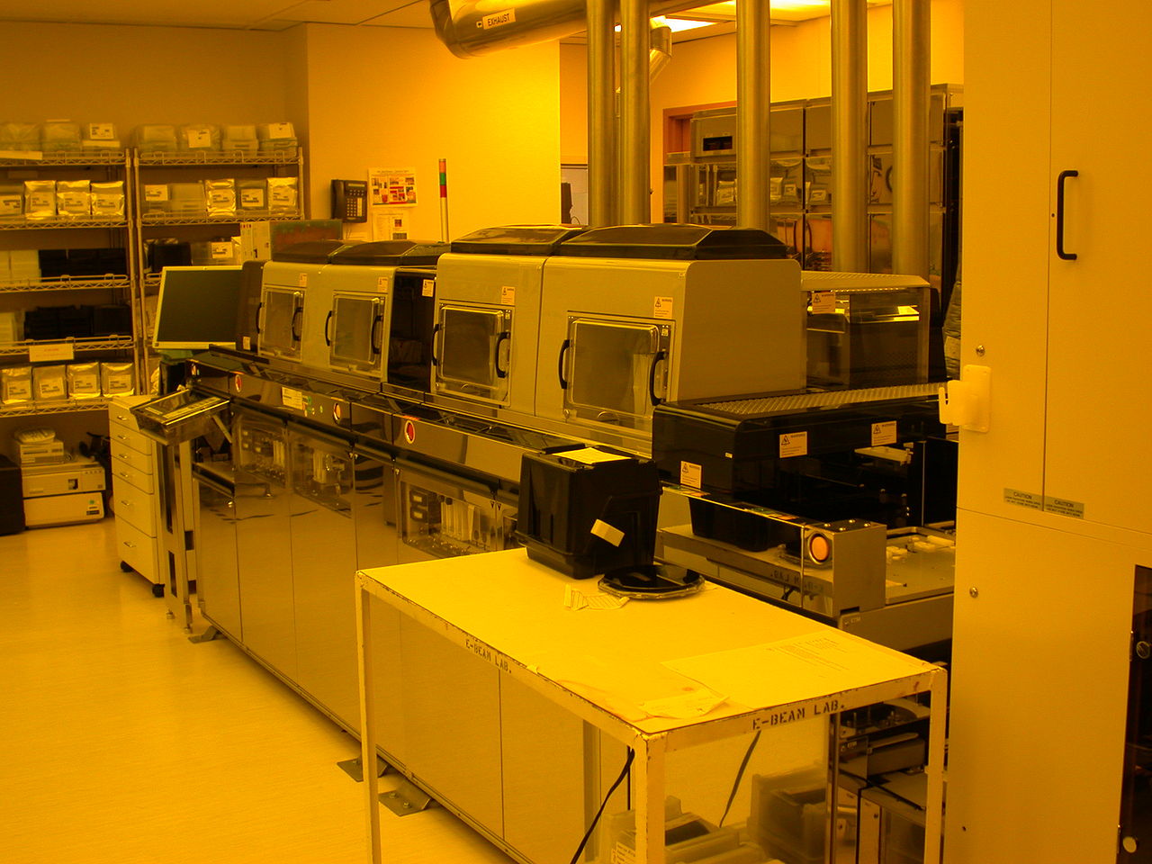
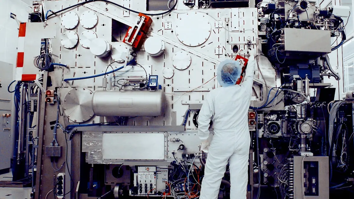
ASML builds the tool behind the most advanced chips
ASML makes the world's most advanced chipmaking tools. Its leading systems use extreme ultraviolet light, or EUV, to print extraordinarily small circuit patterns on silicon wafers.
TSMC uses ASML's EUV machines to manufacture leading-edge chips designed by companies around the world.
The Dutch achievement combines optics, lasers, sensors, mechatronics, software, and a global supplier network into one reliable production system.
Huawei became a global leader in 5G telecom equipment, supplying radios, antennas, base stations, and networking systems used to carry mobile data.
Its success required difficult engineering across radio communication, signal processing, networking, semiconductors, software, and equipment that must operate reliably at enormous scale.
China demonstrated advanced capability in an entire communication system, not only in one component.
Further reading: Eva Dou, House of Huawei, a reported history of the company and its geopolitical importance.
Specialization creates efficiency, but also dependence. A disruption at one hard-to-replace link can affect economies, public services, and national security.
Inside a phone is not merely silicon. It is decades of accumulated knowledge, institutions, rivalry, cooperation, supply chains, and choices about who controls production.
Back to our computer
Use one signal to control another path
control = 0→
channel unavailablesource output
→output = 0
control = 1→
channel availablesource output
→output = 1
This is a functional model, not a physical cross-section. A small control signal changes whether another electrical path conducts.
From here onward, we hide the device physics and reason with two states: 0 and 1.
Further study:NPTEL Basic Electronics by Prof. M. B. Patil, IIT Bombay, covers electronic devices and semiconductor fundamentals.
Logic gates
Connect switches to make a tiny decision-maker
Input signals0 or 1
→
Gatefixed rule
→
Output signal0 or 1
A logic gate hides its transistors and exposes only inputs, an output, and a rule.
How can we describe that rule precisely without discussing the internal transistors?