Lecture 10 | Sequential Logic
Program Counter
Remembering which instruction comes next.
Program Counter
Why Does a Computer Need a Counter?
Normal executionMove to the next instruction: PC = PC + 1.
JumpLoad a different instruction address into the PC.
Restart or waitReset to 0, or hold the same instruction address.
Program Counter
The PC Interface
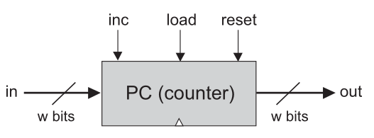 Program Counter symbol
Interface
- Data input
in[16], used when loading a new address.- Control inputs
inc, load, and reset.- Output
out[16], the currently stored instruction address.
Each control input is one bit. They decide whether the next stored value is zero, the external input, the incremented value, or the old value.
Program Counter
The PC Contract
Specification- Chip name:
- PC
- Inputs:
in[16], inc, load, reset- Outputs:
out[16]- Function:
if reset(t-1) then
  out(t) = 0
else if load(t-1) then
  out(t) = in(t-1)
else if inc(t-1) then
  out(t) = out(t-1) + 1
else
  out(t) = out(t-1)
Symbol
Control Priority
Why Priority Is Necessary
What should happen when more than one control bit is 1?
Examplereset=1, load=1, and inc=1
Contract saysreset wins, so the next output is 0.
Priority orderreset > load > inc > hold
Priority is part of the specification, not merely an implementation choice.
Program Counter
Example: Tracing the PC
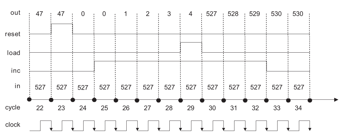 Example behavior of the Program Counter over time
Use the priority order reset > load > inc > hold to read each cycle.
Exercise 1
Trace the PC
Assume the PC starts with out=47. Fill the output after each cycle.
| cycle | in | reset | load | inc | out after cycle |
|---|
| 1 | 527 | 0 | 0 | 0 | 47 |
| 2 | 527 | 1 | 0 | 0 | 0 |
| 3 | 527 | 0 | 0 | 1 | 1 |
| 4 | 527 | 0 | 1 | 1 | 527 |
| 5 | 800 | 1 | 1 | 1 | 0 |
Sequential Design
Constructing the PC
Use known chips to compute candidate next values, then select the one mandated by the control priority.
Registerstores the current PC value.
Mux16 / Mux4Way16selects among hold, increment, load, and reset candidates.
Control logicenforces reset > load > inc > hold.
Exercise 2
Control the Internal Register Load
The internal Register changes only when its own load input is 1. When must the PC force that internal load to 1?
internalLoad = ?
internalLoad = reset OR load OR inc
If all three controls are 0, the PC holds its previous value, so the internal Register need not load.
Exercise 3
Debug a Broken PC
A proposed PC gives inc priority over load. Find a counterexample.
Inputsin=200, load=1, inc=1, reset=0
The specification says load wins, so the next output must be 200. The broken design would output 11. Therefore the priority order is wrong.
Sequential Design
Sequential HDL and Simulation
Inside the cycleinputs may changeCombinational logic may take time to settle.
At the boundarystate commitsDFF-based chips capture the value that should be remembered.
In simulator tests, tick and tock let us observe this clocked behavior.
Exercise 4
Predict Before Simulation
A Bit starts with out=0. Predict the observed output.
| cycle | in | load | out after cycle |
|---|
| 1 | 1 | 0 | 0 |
| 2 | 1 | 1 | 1 |
| 3 | 0 | 0 | 1 |
| 4 | 0 | 1 | 0 |
Chapter Summary
One Hierarchy, Built Bottom-Up
Memory path- DFF
- Bit
- Register
- RAM8
- RAM64
- RAM512, RAM4K, RAM16K
Counter path- Register stores the current value
- Inc16 computes the next value
- Selection logic chooses reset, load, inc, or hold
- PC becomes the controlled counter
Exercise 5
Chapter Tutorial Questions
1Can two writes to different RAM addresses interfere? Explain using load routing.
2A RAM has 2048 words of 16 bits. Find address width and total capacity in bytes.
3Design a two-register memory using Registers, DMux, and Mux16.
4Why can a sequential chip tolerate temporary unstable combinational values within a cycle?
5If a 16-bit PC at 32767 increments, what bit pattern follows? Interpret it as unsigned and signed.
6Write an HDL plan for PC reset and load priority using Mux16 chips.
Laboratory Preparation
Build the Chapter 3 Chips
1Bit
2Register
3RAM8
4RAM64
5RAM512
6RAM4K
7RAM16K
8PC
Allowed building blocksUse primitive DFF, chips gradually built in this lab, and chips from previous chapters. Test every level before building on top of it.
Summary of This Lecture
Program Counter
StateThe PC remembers the instruction address.
ControlIt can reset, load, increment, or hold.
Priorityreset > load > inc > hold.
Chapter ideaA one-cycle delay makes feedback, memory, and counters possible.
Next Lecture | Machine Language
Lecture 11: Machine Language
Now that the hardware can compute and remember, we can ask how programs speak to the machine.