Clock and Time
What Happens During a Cycle?
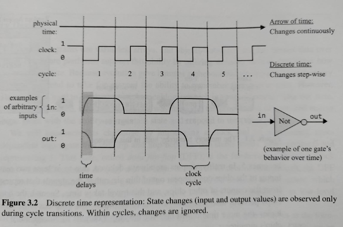
Reading the figure
- During a cycle
- Combinational logic reacts to the input values it currently receives.
- At a boundary
- Sequential chips commit their stored outputs.
- Why it matters
- Without clock cycles, phrases like "previous input" and "next output" are ambiguous.
Data Flip-Flop
Data Flip-Flop (DFF)
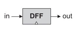
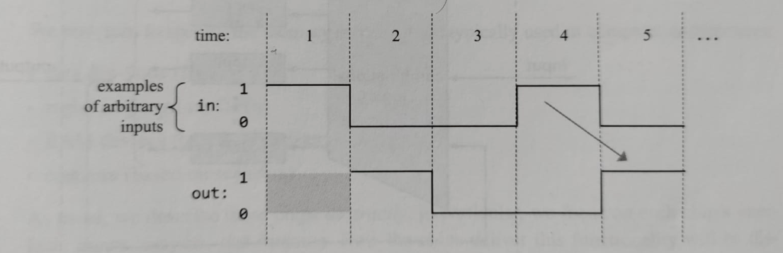
A Data Flip-Flop (DFF) is the primitive one-bit time delay used by the simulator.
Specification
- Chip name:
- DFF
- Inputs:
in- Outputs:
out- Function:
out(t)=in(t-1)- Implementation:
- Primitive, supplied by the simulator.
Sequential Logic
Combinational Logic and Sequential Logic
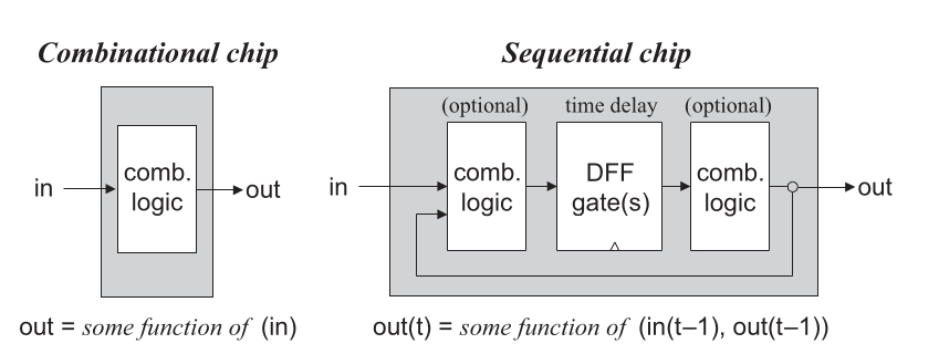
Combinational chip
out = f(in)Output depends only on current input values.
Sequential chip
out(t) = f(in(t-1), out(t-1))Output can depend on earlier input values and earlier stored state.
Registers
What Is a One-Bit Register?
A one-bit register is a storage cell that remembers one bit until we explicitly load a new bit.
Required behavior
- Read
- The output continuously shows the currently stored bit.
- Hold
- If
load=0, keep the stored bit even ifinchanges. - Load
- If
load=1, store the input bit at the next clock boundary.
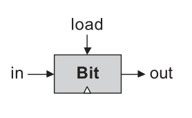
Terminology
The Hack platform calls this one-bit register chip Bit.
Register
Building a One-Bit Register: First Try
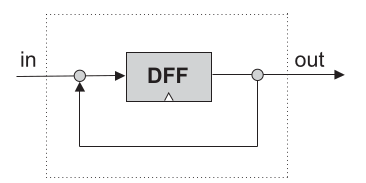
- It is not clear how we will ever load this device with a new data value.
- There is no means to tell the DFF when to draw its input from
inand when fromout. - Internal pins must have fan-in 1: each internal pin must be fed from a single source only.
Register
Correct Implementation of a One-Bit Register
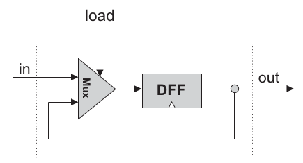
- Introduce a multiplexor to resolve the input ambiguity.
- The Mux select bit becomes the register's
loadbit. - If
load=1, the register starts storing the new value onin. - If
load=0, the register keeps storing its internal value.
Registers
The Bit Contract
Specification
- Chip name:
- Bit (1-bit register)
- Inputs:
in, load- Outputs:
out- Function:
- If
load(t-1)thenout(t)=in(t-1); elseout(t)=out(t-1).
Read
Probe out. This does not require load=1.
Put the new bit on in and set load=1. The value appears next cycle.
Exercise 1
Trace a Bit
Use the Bit behavior: load=1 loads at the next boundary; load=0 holds the old value. Assume the stored bit starts as 0.
| Cycle | in | load | out after cycle |
|---|---|---|---|
| 1 | 1 | 0 | 0 |
| 2 | 1 | 1 | 1 |
| 3 | 0 | 0 | 1 |
| 4 | 0 | 1 | 0 |
| 5 | 1 | 0 | 0 |
Registers
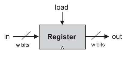
The Register Contract
Specification
- Chip name:
- Register
- Inputs:
in[16], load- Outputs:
out[16]- Function:
- If
load(t-1)thenout(t)=in(t-1); elseout(t)=out(t-1). - Comment:
- The assignment is a 16-bit operation.
Example
| cycle | in[16] | load | out after cycle |
|---|---|---|---|
| 1 | 0000...0011 | 1 | 0000...0011 |
| 2 | 1111...1111 | 0 | 0000...0011 |
| 3 | 1111...1111 | 1 | 1111...1111 |