Lecture 9 | Sequential Logic
Random Access Memory
Selecting one word among many.
Memory
From One Register to Many
RegisterStores one 16-bit word.
Memory bankAn array of fixed-width Registers.
Two parametersWidth is bits per word. Size is number of words.
Random Access
What Does Random Access Mean?
Random access means any word can be accessed directly, in the same way, regardless of which word was accessed previously.
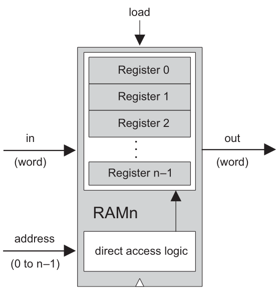 Conceptual view of RAM
Not random in this senseunpredictableThe memory does not choose a location randomly.
Random access meansdirect selectionThe address selects the word we want to read or write.
Random Access
Addresses
Each word is selected by a binary address. If a memory has 2^k words, it needs k address bits.
RAM88 words = 2^3 words, so the address has 3 bits.
Example address101 selects word number 5.
ImportantAddresses are implemented by selection logic. They are not labels physically written on the registers.
Exercise 1
Address Capacity
Find the number of address bits required for each memory.
| Memory | Number of words | Address bits |
|---|
| RAM8 | 8 | 3 |
| RAM64 | 64 | 6 |
| RAM512 | 512 | 9 |
| RAM4K | 4096 | 12 |
| RAM16K | 16384 | 14 |
A 10-bit address can select 2^10 = 1024 locations.
Memory
The RAM Contract
Specification- Chip name:
- RAMn
- Inputs:
in[16], address[k], load- Outputs:
out[16]- Read:
out(t)=RAM[address(t)](t)- Write:
- If
load(t-1), then RAM[address(t-1)](t)=in(t-1).
Specific Hack RAM chips| Chip | words | address bits |
|---|
| RAM8 | 8 | 3 |
| RAM64 | 64 | 6 |
| RAM512 | 512 | 9 |
| RAM4K | 4096 | 12 |
| RAM16K | 16384 | 14 |
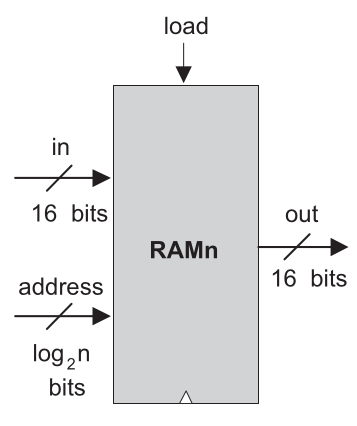 Symbol
Memory
Read Now, Write Next Cycle
ReadcombinationalChanging address selects the current word immediately.
WriteclockedIf load=1, the selected Register commits to in at the next cycle boundary.
This asymmetry is the main timing idea for RAM.
Exercise 2
Trace Reads and Writes
Initial memory: address 00=7, 01=2, 10=9, 11=4. Fill out during cycle and update memory after each cycle.
| cycle | address | in | load | out during cycle |
|---|
| 1 | 01 | 8 | 0 | 2 |
| 2 | 10 | 5 | 1 | 9 |
| 3 | 10 | 0 | 0 | 5 |
| 4 | 00 | 3 | 1 | 7 |
After cycle 4, the changed words are address 10=5 and address 00=3.
RAM Construction
Building RAM8
RAM8 contains eight 16-bit Registers plus direct-access logic.
Question 1How does load reach only the selected Register?
Use: DMux8Way.
Register 0Register 1Register 2Register 3Register 4Register 5Register 6Register 7
Question 2How does only the selected Register reach out?
Use: Mux8Way16.
Exercise 3
Complete the RAM8 Diagram
1Add a DMux8Way to route load.
2Add a Mux8Way16 to select the output.
3Connect address[0..2] to both selection circuits.
4Write the corresponding HDL connection plan.
PARTS:
  DMux8Way(in=load, sel=address, a=l0, b=l1, ..., h=l7);
  Register(in=in, load=l0, out=o0);
  ...
  Register(in=in, load=l7, out=o7);
  Mux8Way16(a=o0, b=o1, ..., h=o7, sel=address, out=out);
Hierarchical Addressing
Building RAM64 from RAM8
A six-bit RAM64 address can be read as abc def.
Upper three bits: abcSelect one of eight RAM8 chips.
Lower three bits: defSelect one Register inside the chosen RAM8.
Exercise 4
Find the Physical Path
For each RAM64 address, identify the RAM8 bank and the Register inside that bank.
| RAM64 address | bank bits | offset bits | path |
|---|
000101 | 000 | 101 | bank 0, register 5 |
011110 | 011 | 110 | bank 3, register 6 |
111001 | 111 | 001 | bank 7, register 1 |
Hierarchical Addressing
Recursive Memory Construction
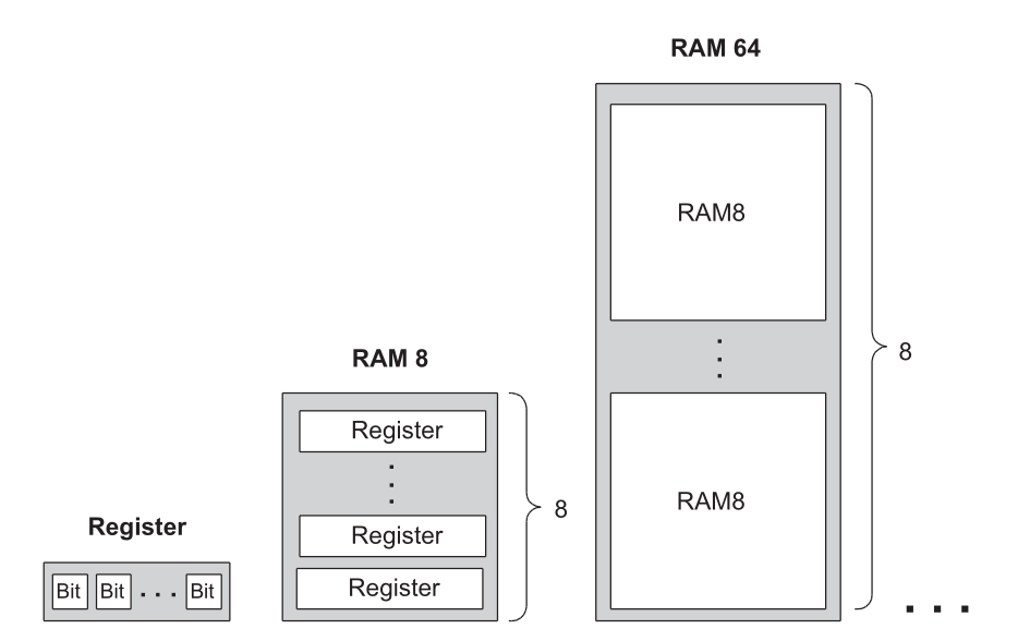 Recursive ascent from registers to RAM
Repeated idea
- Register to RAM8
- Use eight Registers and direct-access logic.
- RAM8 to RAM64
- Use eight RAM8 chips and split the address into bank bits and offset bits.
- Larger RAM chips
- Repeat the same construction recursively.
Exercise 5
Split the Address
How should the address bits be divided at each construction step?
| Build | address bits | select subchip | inside subchip |
|---|
| RAM512 from RAM64 | 9 | upper 3 | lower 6 |
| RAM4K from RAM512 | 12 | upper 3 | lower 9 |
| RAM16K from RAM4K | 14 | upper 2 | lower 12 |
Summary of This Lecture
Random Access Memory
Registersstore 16-bit words.
Addressesselect which word is read or written.
Read/write timingread is immediate; write commits next cycle.
Hierarchylarge RAM chips are built recursively from smaller RAM chips.
Next Lecture | Program Counter
Lecture 10: Program Counter
A stateful chip that can hold, increment, load, or reset a number.